When does draw a rectangle not draw a rectangle, but select items? When you're using #KiCad of course.
(I'm likely using it wrong, and will be looking up at the docs, but I kinda expect that when I click on an icon which tool tip says draw rectangle, I expect it to draw, not select).
Thanks roboya:
Sorry guys, I found the trick: I was clicking a point and dragging the mouse. The right way to do it
is: click & release first point, move to second point (diagonal), click & release second point.
So, I get that #KiCad can't have symbols and footprints for every component ever in their default library, but some of the things they've chosen to include can be a little confusing when compared against what they haven't chosen to include. Here's an example:
There are symbols for the TC74HC00 (quad NAND gate) and TC74HC08 (six channel inverter) series of chips, but none for the TC74HC04 (quad AND gate). Sure, the 74HC00 symbol can fairly trivially be edited into a 74HC04, but still... Am I missing something here?
Fortunately, for this particular board I was able to do some boolean magic with a single 74HC00, so it's a moot point.
@me Since these libraries are mostly made by hobbyists as needed, there are lots of gaps. If you can afford the time, feel free to contribute your symbols over at https://gitlab.com/kicad/libraries/kicad-symbols/
Are there any good tutorials out there for #kicad? I am quite familiar with schematics, just need to wrap my head around how to draw them a bit better using #kicad, and learn the various features of #kicad
@trevorflowers Oh no. Do you have another board order to place? 😭
(I'll never forget the time I forgot to reflow my ground plane after Just One More Tweak, didn't re-run ERC, and ended up with VCC wired straight to GND on the boards I had made...)
Expecting some circuit boards today maybe. Exciting - my first use of #KiCad right through to actually producing PCBs, though I've worked up a few schematics in the past, and one other PCB layout.
Haven't bought any new boards for a project in a couple of years either, so it's nice for that reason too.
This design is a pretty simple amalgam of a bunch of peripheral elements attached to a new-to-me module that uses an ATMega4808 processor.
That module is much like the Arduino Nano Every (4809) but much cheaper ($5 vs $21) though poorly documented and more convoluted to use.
Also I'm liking the #KiCad 3D viewer too, but I have to discover how to add solid-models for the 3D view renderings. (Fingers crossed that it's just an .stl file reference).
Yay - my circuit boards arrived yesterday evening.
Have been playing with getting a good fit into my unusually-shaped enclosure and think I've managed it. A hot soldering iron is very useful for sculpting changes in the 3Dprinted shell.
Accidental fumes from PLA are thankfully not too nasty – a bit sweet smelling.
Dear @kicad: I'm pretty sure I'm ignorant to why some decisions were made regarding the start screen, yet it makes no sense to me. Is there any explanation why things are not how I put in the attached image? Thanks! Regardless, still a wonderful tool (that I absolutely love). Cheers! #kicad#ux Edit: I mixed "screen state" with "screen space" in the image. 👅
@dmian@kicad Honestly, I don't know much about kicad's source code (I'd love to dive in, but can't seem to motivate myself enough to learn C++). But I feel like I have heard the legacy code thing a lot when people talk about certain seemingly obvious kicad UI improvements. So from my very surface level understanding of the program, I feel like that part of the code could use some love. But I'd imagine that'd be a crazy big project I couldn't even begin to imagine the scope of.
@dmian@kicad I wish I had the time, energy and skill to throw at a project like that but I am just a simple electrical engineer with a small amount of programming knowledge.
Anyone have an open-source #KiCad PCB design that 3D renders with components and looks at least moderately interesting? Doesn't need to be anything specific. I just need a 3D model of a PCB for a demo of a simple program.
I've tried using some projects linked from the KiCad web site, but even for the ones where a rendering is shown on the web site, the only renderings I can get have no components, just the bare PCB. I must not have the necessary libraries.
Thanks!!!
@brouhaha that does seem kinda not right though. maybe when you installed KiCad 8.0 it ported some settings back from 6.0 or something and didn't set up your 3D paths right?
I'm guessing on Linux they should be under something like /share/kicad/3dmodels (or /usr/share). if not try searching your disk for a file called C_Axial_L3.8mm_D2.6mm_P15.00mm_Horizontal.wrl
Ugh, an intensive day with too much sitting, fully immersed in circuit work.
The ramp up with #KiCad tools was very smooth. I didn't find any roadblocks in #schematic capture, part coding, #PCB layout, nor cleaning up DRCs. The tools have come a long way since my last use in 2021! Pleased!
A scan through manufacturability tomorrow and the full cycle is complete. Yay #FOSS.
It's been a couple of years since I last used #KiCad. I had just finally given up on #EagleCAD in spite of my large library personal parts, but it was time.
A bit of a learning curve, but I got there, and was happy with KiCad's capabilities. Now I guess I'll ramp up from scratch again. Ugh. Hope it comes back quickly.
Checking versions, I have 5.1.12 and see the latest is… gulp 8.0.2. Well, I'm ramping up from dim recollections anyway, so it shouldn't add much extra effort.
@trevorbattle yeah if I remember correctly, I didn't upgrade beyond the version where you needed a live connection to an AutoDesk account to use the thing, that was a deal breaker.
Are you working with an KiCad or Fritzing and want to support them? Select the Development Contribution option during checkout. This will add a €2 charge to your order, we will double this and transfer it to the developer of the tool you used.
Unsere letzte Folge ist zwar schon etwas her, aber wer sie noch nicht gehört hat: Wir sprachen u.a. über #KiCad 8.0 – #Electronics#Design#Automation mit vielen
Woohoo I am a KiCad master now! Or at least I know enough to default to it instead of Eagle. Finally. Plus I found a neat capacitive touch sensor chip that I got working in CircuitPython and Arduino on a Pico #KiCad#CircuitPython#RaspberryPiPico#CapacitiveTouch
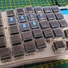
Watch out, I'm a hardware designer now! My first board is here and it works!
Super happy with the "ambient light" effect:) There's one LED shining at the back into the hand, and another behind the screen, giving the impression of light passing through the PCB. Quite mesmerizing.
I still need to put side LEDs on (one for each of the touch pads), but those tiny SK6812-4020 turned out to be way beyond my amazing soldering skills 😅
First batch QC checked and shelled 🤓 Case is snap fit and is sturdy, there's a tolerence spacing but it's not even shaking, only to allow stronger presses and a way to open it in case it's needed. The item looks even better in hand.
#KiCAD is giving me a run for my money today. 6 hours in, and I haven't found a good workflow for reusing a schematic and layout between multiple projects ("design blocks" in other CAD).
So far, my best bet is a time-consuming and fragile process: put several projects in the same folder, link hierarchical sheets, and copy-paste the layout from one project to the others.
@stargirl@azonenberg@mntmn , seems like all of you make complex hardware in kicad and have likely run into this problem?
Does not work between projects unless they have matching sheet hierarchy
Does not copy intersecting traces past the first junction
...which makes it useful if you have a simple copy-modify project pattern and a simple repeating block that can be auto-routed, but not useful for sensitive layouts like switching converters or microcontrollers.
I'm pretty excited by this news from the #KiCAD 8 announcement page: "With the help of 8 new librarians joining the effort, the library gained over 1500 new symbols and 760 footprints, and had thousands of updates to fix or improve existing parts." https://www.kicad.org/blog/2024/02/Version-8.0.0-Released/
Did you know that there is a awesome wiki for the #KiCad library?
It has pages for footprint and symbol design, with lots of background info regarding the KLC rules and IPC standards.
With lots of tips and tricks to the creation and submission for the official library.
The newest addition is a page that has Pin1 silkscreen markers that you can copy to the clipboard and paste inside KiCad.